Global 3D Semiconductor Packaging Market Size, Share, Trends, Industry Statistics Report, By Technology (3D Through SILICON VIA (TSV), 3D Package on Package (PoP), 3D Fan Out, 3D Wire Bonded, and Other (Flip Chip and Hybrid)); by Material (Organic Substrate, Bonding Wire, Lead Frame, Encapsulation Resin, Ceramic Package, Die Attach Material, and Others); Regional Analysis (North America - U.S, Canada, Other) (Asia-Pacific - India, Japan, China, South Korea, Japan, Australia, and Other) (Europe - U.K., Germany, Netherlands, Lithuania, Austria, Belgium, Poland, Sweden, Spain, France, Russia and Other) (Middle East - Saudi Arabia, UAE and Africa - South Africa, Zimbabwe and RoW) - Global Industry Insights, Trends and Forecast, 2019-2025
Report Format : PDF
Published Date : Oct-2018
Pages : 190
Report ID : VSR001193
Report Format: PDF
Published Date: Oct-2018 | 190 Pages | Report ID: VSR001193
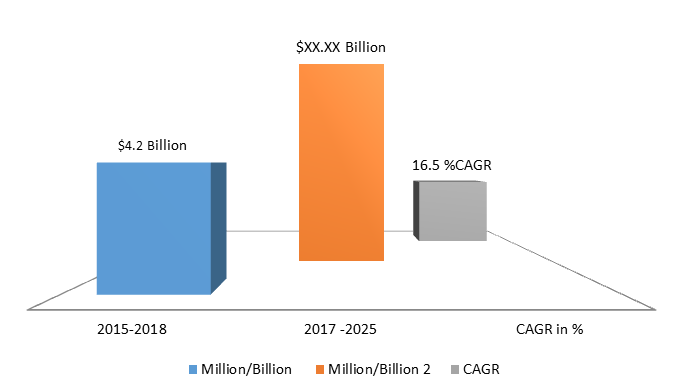
Global 3D Semiconductor Packaging Market Size is estimated to expand rapidly in coming years, at a CAGR of 16.5 % from 2018 to 2025. In 2017, the global market valuation was USD 4.2 billion, and it is anticipated to be greater than USD xx.xx billion by 2025. Three-dimensional integrated circuits are produced by stacking of silicon wafers and interconnecting the wafers vertically through Silicon Vias (TSVs), which further empowers them to carry on as a solitary gadget at lesser power when contrasted with customary innovation.
Developing interest for gadgets with a higher limit just as lesser storage is one of the key components expected to drive the DRAM and NAND showcase. Besides, with the rising interest for customer electronic items, offers of MEMS gadgets just as picture sensors are foreseen to observe significant development over the estimate time frame, in this manner expanding the appropriation of 3D ICs in changed gadgets. Expanding interest for tablets, wearable gadgets, low-end cell phones, and other associated customer products, wherein the key players underscore on more up to date bundling advances, is required to drive market development. Three-dimensional integrated circuits bundling utilizing Silicon-Vias innovation are utilized to incorporate semiconductor advances into miniaturized scale electronic modules and stack diminished semiconductor chips. The transfer speed necessities for systems administration gear just as capacity limits are relied upon to develop at a noteworthy rate. Silicon on insulator wafers is favored for 3D IC creation, wherein it helps in the decrease of undesirable warmth generation. Geographically, the market in North America held largest share in the global market.
Global Market Growth Opportunities (Revenue, Growth) By 2017-2025
This global market study report analysis offers in-depth insights, revenue details, and other vital information regarding the global 3D semiconductor packaging market, and the various trends, drivers, restraints, opportunities, and threats in the target market till 2025. The report offers insightful and detailed information regarding the various key players operating in the market, their financials, supply chain trends, technological innovations, key developments, apart from future strategies, acquisitions & mergers, and market footprint. The global 3D semiconductor packaging market report has been segmented on the basis of type, application, and region. It includes the estimation of the market size, in terms of value, with respect to 4 main geographies, namely, North America, Europe, APAC, and RoW.
Segment Analysis
By Technology Insights: On the basis of technology, global 3D semiconductor packaging market has been segmented into 3D through SILICON VIA (TSV), 3D package on package (PoP), 3D Fan Out, 3D Wire Bonded, and other. Other segment is further bifurcated into Flip Chip and Hybrid. Among which 3D package on package (PoP) is expected to witness high growth in forecast period. Application processors utilizing advanced innovations are relied upon to be littler and quicker in examination with chip bundled according to customary setups. 3D innovation aides in expanding data transfer capacity, improving execution just as power productivity. Three-dimensional semiconductor advances help in bringing down hazard just as decreasing cost, subsequently making it a feasible arrangement crosswise over changed applications.
By Material Insights: On the basis of material, global 3D semiconductor packaging market has been segmented into organic substrate, bonding wire, lead frame, encapsulation resin, ceramic package, die attach material, and others. Among which organic substrate segment is expected to witness high boost in the global market of 3D semiconductor packaging. This innovation incorporates noteworthy advantages, for example, heterogeneous reconciliation, wherein the circuit layers are based on various wafers with shifted forms. Shorter interconnect just as circuit security is additionally key advantages given by the 3D innovation. Three-dimensional incorporated circuits wires have higher capacitance than traditional wired innovations. Moreover, touchy circuits are separated into various layers for the clouding capacity of each layer. Three-dimensional ICs advancements are likewise occupied with offering more prominent chip availability in examination with customary arrangements.
Regional Analysis
The 3D semiconductor packaging market is divided into regions that are North America - U.S, Canada, Other; Asia-Pacific -India, Japan, China, Australia, Other; Europe - UK, Russia, France, Brazil, Other; Middle East and Africa. Every region analysis details in sense of growth, revenue, volume, challenges, and opportunities with the regional and global key players.
Topographically, the North America area is the most astounding developing locale in the worldwide market of the 3D semiconductor bundling market. The Market's development in the region is driven by the solid development of the hardware business in nations, for example, the US, Canada, and Mexico. American shoppers are inclining towards scaled-down electronic gadgets that are smaller yet don't settle on power. What's more, the quick selection of top of the line electronic gadgets and the ascent of AI and man-made reasoning (AI) are different variables that possible advance the utilization of 3D bundling for different semiconductor parts.
Overall supply for 3D semiconductor packaging has been extremely large in Asia Pacific and this region is anticipated to guide the industry over the forecast period in terms of development pace. A lot of makers in the worldwide 3D semiconductor bundling business sector hold limits in the Asia Pacific, enabling it to be the main locale in the market as of now. Europe is anticipated to maintain steady growth in the global 3D semiconductor packaging market.
Global 3D Semiconductor Packaging Market Size, Share Analysis by Region 2017
Global 3D Semiconductor Packaging Market Study Objective
1. To forecast the market size of 3D semiconductor packaging market, along with describing and defining the market, in terms of volume and revenue as well as market opportunities for stakeholders, in order to provide a competitive landscape for global market players.
2. Market analysis and forecast of 3D semiconductor packaging market on the basis of region, substrate, and application or end-use industry. To profile major market players, and to analyze their market shares and essential competencies comprehensively.
3. To analyze and elaborate significant factors that will have a major impact on the growth of 3D semiconductor packaging market, such as drivers, restraints, challenges, and opportunities.
4. The regional analysis of 3D semiconductor packaging market, to induce market size of five global major regions, which include, Europe, North America, South America, Middle East & Africa, and the Asia Pacific.
5. Strategic analysis of micro markets, in terms of individual prospects, opportunities, growth trends and their involvement in the overall market.
6. To provide detailed analysis of competitive and strategic developments in the 3D semiconductor packaging market like a new product launch, partnership & agreement, investment & expansion, and company merger & acquisitions.
Key Players Landscape
Amkor Technology Inc., Jiangsu Changjiang Electronics Technology Co. LTD., International Business Machine Corporation (IBM), Qualcomm Technology Inc., Intel Corporation, Taiwan Semiconductor Manufacturing Company Ltd., Stmicroelectronics N.V., Siliconware Precision Industries Co., Ltd (SPIL), Suss Microtec AG., and ASE Group are some of the key players in the market of 3D semiconductor packaging.
Global 3D Semiconductor Packaging Market Study Report Offer You!
The global 3D semiconductor packaging market study report gives an idea about market size, share, stock, equity, investment and total price analysis. Also, the report provides comprehensively industry insights with all major factors such as market credit, allocation, demand, distribution, market scope, key players, end user & applications, provisions, livestock, commodities and industry economics analysis, future growth & forecast. The global market report includes all depth data like pre-market emphasis, market survey, market investment, industry advice, portfolio, finance, access, trade, market exploration, industry review and market predication & projection to develop effective strategies for optimizing their market position.
Enquiry for Table of Content
Global 3D Semiconductor Packaging Market Size, Share, Trends, Industry Statistics Report, By Technology (3D Through SILICON VIA (TSV), 3D Package on Package (PoP), 3D Fan Out, 3D Wire Bonded, and Other (Flip Chip and Hybrid)); by Material (Organic Substrate, Bonding Wire, Lead Frame, Encapsulation Resin, Ceramic Package, Die Attach Material, and Others); Regional Analysis (North America - U.S, Canada, Other) (Asia-Pacific - India, Japan, China, South Korea, Japan, Australia, and Other) (Europe - U.K., Germany, Netherlands, Lithuania, Austria, Belgium, Poland, Sweden, Spain, France, Russia and Other) (Middle East - Saudi Arabia, UAE and Africa - South Africa, Zimbabwe and RoW) - Global Industry Insights, Trends and Forecast, 2019-2025
Enquiry for Methodology
Global 3D Semiconductor Packaging Market Size, Share, Trends, Industry Statistics Report, By Technology (3D Through SILICON VIA (TSV), 3D Package on Package (PoP), 3D Fan Out, 3D Wire Bonded, and Other (Flip Chip and Hybrid)); by Material (Organic Substrate, Bonding Wire, Lead Frame, Encapsulation Resin, Ceramic Package, Die Attach Material, and Others); Regional Analysis (North America - U.S, Canada, Other) (Asia-Pacific - India, Japan, China, South Korea, Japan, Australia, and Other) (Europe - U.K., Germany, Netherlands, Lithuania, Austria, Belgium, Poland, Sweden, Spain, France, Russia and Other) (Middle East - Saudi Arabia, UAE and Africa - South Africa, Zimbabwe and RoW) - Global Industry Insights, Trends and Forecast, 2019-2025

Why Choose Veracious Statistics Research ?
Save Your Time
Cost-Effective Services
Wide Range of Reports
World Class Market Research
100% Customer Satisfaction
24/7 Customer care Support
Any more questions?
Get in touch with us quickly and easily. We are happy to help!
Do you still have questions?
Feel free to contact us anytime using our contact form.
Contact us

 2024 © Veracious Statistics Research All Rights Reserve